How NVMe Host Memory Buffer Works in Client DRAM-Less SSDs
Learn how the NVMe Host Memory Buffer mechanism allocates host DRAM via PCIe DMA to accelerate Flash Translation Layer lookups without on-drive memory chips.
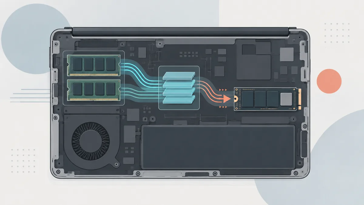
Client solid-state drives (SSDs) face a persistent hardware tradeoff between bill-of-materials cost, thermal envelopes, and sustained random I/O throughput. Solid-state storage controllers rely on dynamic random-access memory (DRAM) to store the Flash Translation Layer (FTL) logical-to-physical (L2P) address mapping tables. In client devices such as ultra-thin laptops, handheld PC gaming consoles, and budget consumer desktops, omitting dedicated onboard DRAM chips lowers manufacturing expense and simplifies single-sided PCB layouts.
However, running an SSD without volatile working memory forces the controller to retrieve address mapping tables directly from NAND flash, creating severe latency bottlenecks. To eliminate this penalty without adding on-drive DRAM, the NVM Express consortium introduced the NVMe Host Memory Buffer (HMB) feature in NVMe Specification 1.2.
The NVMe Host Memory Buffer feature allows a DRAM-less storage controller to borrow a small slice of host system DRAM—typically between 16 MiB and 128 MiB—over the PCIe bus. By executing direct memory access (DMA) transactions across the Root Complex, the SSD controller caches mapping entries in host memory, achieving random I/O performance that rivals drives equipped with dedicated onboard LPDDR4 chips.
The Flash Translation Layer Problem in DRAM-Less SSDs
NAND flash memory cannot overwrite existing data in place. Storage controllers must write data in pages (typically 16 KiB) and erase data in large multi-megabyte blocks. The Flash Translation Layer abstracts these non-linear physics from the operating system by maintaining a 1:1 or 4 KiB-granular Logical Block Address (LBA) to Physical Block Address (PBA) mapping table.
+-------------------------------------------------------------------------+
|                  4 KiB Logical-to-Physical (L2P) Mapping                |
|                                                                         |
|  Drive Capacity : 1 TiB (1,099,511,627,776 Bytes)                       |
|  Page Granularity: 4 KiB (4,096 Bytes) -> 268,435,456 Logical Entries  |
|  Entry Width     : 4 Bytes (32-bit PBA pointer)                         |
|  Total L2P Size  : 268,435,456 * 4 Bytes = 1,073,741,824 Bytes (1 GiB)  |
+-------------------------------------------------------------------------+
As drive capacity scales, the total size of the flat mapping table scales proportionally at roughly 1 GiB of DRAM per 1 TiB of NAND flash. Drives with dedicated onboard DRAM store this entire structure in fast volatile memory. When a read command arrives, the controller queries its local DRAM within 50 to 80 nanoseconds to locate the target NAND block, plane, and page.
In a pure DRAM-less controller without HMB, the chip has only 128 KiB to 2 MiB of embedded static RAM (SRAM). This SRAM holds merely a tiny fraction of the active L2P table. When an incoming I/O request misses the controller SRAM cache:
- The controller must issue an internal NAND page read to load the required FTL mapping chunk from flash into SRAM.
- High-density 3D TLC or QLC NAND page read latencies ($t_{R}$) run between 40 µs and 85 µs.
- Only after the mapping page is retrieved can the controller issue the actual data read to the target flash page, adding another 40 µs to 85 µs.
This "double read" penalty doubles random read latency and collapses random 4 KiB read IOPS under heavy multi-threaded workloads. As storage systems adopt asynchronous submission models, such as io_uring vs pread: How Batched NVMe I/O Actually Scales, the absence of an efficient L2P caching tier causes queue buildups and unpredictable tail latencies.
How NVMe Host Memory Buffer Protocol Negotiation Works
The NVMe Host Memory Buffer mechanism solves this bottleneck by turning system RAM into an external L2P cache. The negotiation process occurs entirely at the driver layer during OS boot or PCIe enumeration.
Host OS Driver (Kernel)                         NVMe Controller
       |                                                |
       |--- 1. Identify Controller (Admin Opcode 0x06)->|
       |<-- 2. Identify Response (HMPRE, HMMIN) --------|
       |                                                |
       |  [Allocates DMA Memory & Builds HMDL Array]    |
       |                                                |
       |--- 3. Set Features: HMB (Admin Opcode 0x09) -->|
       |       Command Dword 11: Enable, Memory Return  |
       |       Command Dword 12: HSIZE (Num of Buffers) |
       |       Command Dword 13: HMDLPA Lower 32-bit    |
       |       Command Dword 14: HMDLPA Upper 32-bit    |
       |<-- 4. Completion Queue Entry (Status Success)--|
       |                                                |
       |  [Controller initiates PCIe DMA read/write]    |
       |<================= PCIe TLPs ==================>|
Identification Phase
During device initialization, the host driver queries the controller with an Identify Controller command (Admin Opcode 0x06). The controller reports its HMB capabilities inside the identify data structure:
- HMPRE (Host Memory Preferred Size): Bytes 272–275 indicate the optimal allocation size in 4 KiB units (e.g.,
0x00010000corresponds to 262,144 pages, or 1,024 MiB for large drives, though budget drives commonly set this to 16,384 pages, or 64 MiB). - HMMIN (Host Memory Minimum Size): Bytes 276–279 define the minimum allocation size the controller needs to initialize HMB functionality (e.g.,
0x00001000= 16 MiB).
If the host operating system cannot grant HMPRE due to memory pressure, it may allocate any value between HMMIN and HMPRE.
Driver Allocation and Descriptor Construction
The host OS allocates physical memory buffers. Because memory allocations of this magnitude often cannot be contiguous in physical memory due to OS memory fragmentation, the NVMe specification mandates a descriptor list: the Host Memory Descriptor List (HMDL).
The Linux kernel driver (drivers/nvme/host/pci.c) prepares an array of descriptors, each describing a physical address chunk and its size. The kernel passes the physical base pointer of this list (HMDLPA) to the controller via the Set Features command (FID 0x0D).
/* NVMe Host Memory Buffer Descriptor entry */
struct nvme_host_mem_buf_desc {
    __le64 addr;    /* Host physical base address (64-bit) */
    __le32 size;    /* Allocation size in 4 KiB memory page units */
    __le32 rsvd;    /* Reserved bits */
};
Feature Activation
To activate HMB, the host writes an administrative Set Features command with Feature Identifier 0x0D:
- Command Dword 11: Bit 0 (
EFLAGS) is set to1to enable the feature. Bit 1 (MR- Memory Return) indicates whether the host is restoring memory preserved across a low-power reset or providing fresh zeroed allocations. - Command Dword 12 (
HSIZE): The total buffer size granted to the device in 4 KiB units. - Command Dwords 13 and 14 (
HMDLPAandHMDLPU): The lower and upper 32-bit physical address pointing to the start of the contiguous descriptor array in host memory. - Command Dword 15 (
HMDLEC): Host Memory Descriptor List Entry Count, informing the controller of the total number of entries in the descriptor array.
Once the controller returns an NVMe status of 0x00 (Success), its internal memory management unit directly accesses the designated host addresses.
Memory Descriptor Lists and PCIe DMA Data Path Architecture
The NVMe controller connects to the PCIe Root Complex via a PCIe Gen4 or Gen5 link. Under HMB operation, the SSD acts as an independent PCIe Bus Master (Requester). It generates PCIe Memory Read (MRd) and Memory Write (MWr) Transaction Layer Packets (TLPs) to access the mapped host memory regions without host CPU intervention.
+------------------------------------------------------------------------------------+
|                                    HOST SYSTEM                                     |
|                                                                                    |
|  +---------------------------+             +------------------------------------+  |
|  |     CPU Cores & Caches    |             |        Host System DRAM            |  |
|  +-------------+-------------+             +-----------------+------------------+  |
|                |                                             |                     |
|                +--------------------+ +----------------------+                     |
|                                     | |                                            |
|                              +------+--+----+                                      |
|                              | Root Complex |                                      |
|                              +------+-------+                                      |
+-------------------------------------|----------------------------------------------+
                                      | PCIe Gen4 x4 Link
+-------------------------------------|----------------------------------------------+
| SSD CONTROLLER                      |                                              |
|                               +-----+------+                                       |
|                               | PCIe Core  |                                       |
|                               +-----+------+                                       |
|                                     | AXI Bus                                      |
|               +---------------------+---------------------+                        |
|               |                                           |                        |
|        +------+------+                             +------+------+                 |
|        | DMA Engine  |                             |  On-Chip    |                 |
|        | (Bus Master)|                             |  SRAM Cache |                 |
|        +------+------+                             +------+------+                 |
|               |                                           |                        |
|               +---------------------+---------------------+                        |
|                                     |                                              |
|                        +------------+------------+                                 |
|                        | Flash Translation Layer |                                 |
|                        +------------+------------+                                 |
|                                     | Flash Channels                               |
|                  +------------------+------------------+                           |
|                  |                  |                  |                           |
|             +----+---+         +----+---+         +----+---+                       |
|             | NAND 0 |         | NAND 1 |         | NAND 2 |                       |
|             +--------+         +--------+         +--------+                       |
+------------------------------------------------------------------------------------+
The Read Path Workflow
When an application issues a random 4 KiB read request, the data path executes through distinct hardware domains:
- Submission: The application submits an NVMe Read Command into the Submission Queue (SQ). The controller pulls the SQ entry via DMA.
- SRAM Tag Check: The controller's embedded core queries its tiny internal SRAM cache to verify if the LBA mapping entry is already locally cached.
- HMB L2P Fetch (Hit in HMB):
- If the entry misses SRAM, the controller checks its internal index to locate which segment of the Host Memory Buffer contains that L2P block.
- The SSD DMA engine formats an outbound PCIe TLP: a 64-bit Memory Read request (
MRd) directed to the physical address in host RAM specified by the correspondingstruct nvme_host_mem_buf_desc. - The Root Complex arbitrates the request, routes it through the system memory controller, reads the 64-byte or 128-byte chunk containing the required L2P mapping metadata, and transmits a Completion with Data (
CplD) packet back down the PCIe link to the SSD.
- Physical Flash Retrieval:
- The controller parses the returned PBA from the
CplDpayload. - The flash controller dispatches an internal command sequence over the Open NAND Flash Interface (ONFI) or Toggle DDR bus to read the NAND flash cell array.
- The controller parses the returned PBA from the
- Data Transfer:
- Once the NAND page arrives at the controller's internal data buffers, the SSD DMA engine initiates an outbound PCIe Memory Write (
MWr) to stream the flash payload directly into the user application's target buffer in host memory. - The controller pushes an entry onto the Completion Queue (CQ) and raises an MSI-X interrupt.
- Once the NAND page arrives at the controller's internal data buffers, the SSD DMA engine initiates an outbound PCIe Memory Write (
When applications stream heavy graphics and geometry assets directly into host memory or GPU storage partitions, as outlined in How DirectStorage Asset Streaming Works in Modern Games, having predictable metadata retrieval times over HMB prevents storage queue stalls.
Latency Profile, Cache Eviction, and Direct Memory Contention
To evaluate the mechanical efficiency of the NVMe Host Memory Buffer, compare the execution latencies across memory hierarchy tiers:
| Cache / Storage Tier | Physical Medium | Access Latency ($t_{access}$) | Bandwidth |
|---|---|---|---|
| SSD Onboard SRAM | Controller SRAM | 1 – 3 ns | > 100 GB/s (Internal AXI bus) |
| Dedicated SSD DRAM | LPDDR4 / DDR4 | 50 – 80 ns | 12 – 25 GB/s (Local memory bus) |
| NVMe HMB Cache | Host DDR4 / DDR5 | 800 – 1,500 ns | 4 – 7 GB/s (PCIe Gen4 link limits) |
| NAND Flash Page Read | TLC / QLC NAND | 40,000 – 85,000 ns | 1.6 – 2.4 GB/s (Per channel bus) |
While reading mapping tables from dedicated onboard DRAM takes under 100 nanoseconds, pulling an FTL segment over PCIe DMA via HMB requires approximately 1.2 microseconds. This accounts for:
- TLP packet serialization and PHY transmission delays ($~150\text{ ns}$).
- PCIe Root Complex traversal and arbitration ($~200\text{ ns}$).
- Host DDR5 memory controller queuing and cell access ($~50\text{ ns}$).
- Return packet completion transmission and reception ($~300\text{ ns}$).
- Internal controller processing and AXI bus routing ($~500\text{ ns}$).
Crucially, 1.2 microseconds is roughly 40 times faster than fetching the mapping table from NAND flash ($50\ \mu\text{s}$). The double-read penalty is virtually erased.
Write-Back Policy and Cache Eviction
Because the Host Memory Buffer resides in volatile host memory that the host OS can reclaim or lose power to instantly, the SSD controller cannot treat HMB as an unbacked write buffer for user data.
- Metadata Exclusivity: HMB is almost universally restricted to caching FTL L2P read mappings and flash block wear-leveling metadata.
- Clean vs. Dirty Tracking: When the host writes new data, the SSD controller updates the translation entry in its internal battery/capacitor-backed SRAM registers or marks the HMB page as dirty.
- Flushing: The SSD controller writes modified translation pages down to dedicated NAND metadata blocks periodically or during an NVMe Flush Command (
Opcode 0x00). If system power drops abruptly, the controller can only guarantee data integrity for LBAs that have had both their user payload and their FTL address entries committed to physical flash cells.
Memory Bus Interference and False Sharing Avoidance
Because the SSD continuously issues PCIe DMA bursts to fetch and update its mapping lines in host memory, system memory controllers must process concurrent memory cycles from both the host CPU and the storage endpoint.
On client platforms running multi-core systems, high I/O transaction rates interacting with host memory tables require the host driver to allocate HMB memory regions along distinct cache line boundaries (typically aligned to 64 bytes or 128 bytes). Misaligned descriptor entries or overlapping DMA buffers can trigger processor cache line invalidation cycles, introducing inter-core traffic stalls akin to the synchronization problems examined in How Cache Line False Sharing Degrades App Performance. The Linux NVMe driver mitigates this by enforcing strict page-aligned allocation boundaries via dma_alloc_coherent().
Failure Modes, Deallocation, and Power States
HMB requires dynamic lifecycle management to prevent data corruption during power state transitions and unexpected bus resets.
Host Memory Reclaim
The operating system may reclaim memory allocated to HMB if host applications encounter severe out-of-memory (OOM) pressure. The driver issues a Set Features command (FID 0x0D) with bit 0 of Dword 11 cleared (EFLAGS = 0).
Upon receiving this disable command, the controller must immediately suspend outbound DMA requests, flush any cached indexing dependent on host addresses, and fall back to its internal SRAM-only translation tier. The host driver then deallocates the DMA buffers:
/* Pseudocode representation of Linux NVMe HMB cleanup */
static void nvme_set_host_mem(struct nvme_dev *dev, u32 size)
{
    struct nvme_command c;
    memset(&c, 0, sizeof(c));
    c.features.opcode = nvme_admin_set_features;
    c.features.fid = cpu_to_le32(NVME_FEAT_HOST_MEM_BUF);

    if (size == 0) {
        /* Disable HMB before freeing memory */
        c.features.dword11 = cpu_to_le32(0); /* EFLAGS = 0 */
        nvme_submit_sync_cmd(dev->ctrl.admin_q, &c, NULL, 0);
        nvme_free_host_mem(dev);
        return;
    }
    /* Normal configuration path ... */
}
Advanced Power Management (APST / D3hot)
Client operating systems dynamically drop PCIe storage devices into low-power Non-Operational Power States (NOPS), such as NVMe Power State 3 or 4, where PCIe link power states shift to L1.1 or L1.2 sub-states. Under these sub-states:
- The PCIe link physical layer disables its transceivers, breaking active DMA communication.
- The SSD controller retains HMB configuration context in its internal registers.
- Prior to entering these states via Autonomous Power State Transitions (APST), the controller ensures that critical dirty mapping records are written out to NAND, as the host system may transition from sleep directly to an unannounced power cut (such as battery depletion).
Conclusion
The NVMe Host Memory Buffer fundamentally changes client storage economics. By using the high throughput and direct DMA mechanics of the PCIe interconnect, HMB bridges the structural performance gap between premium drives with dedicated DRAM and low-cost DRAM-less solid-state designs.
Rather than paying the severe 40-microsecond double-read penalty on cache misses, a modern DRAM-less controller queries the host's system RAM in roughly 1.2 microseconds via PCIe Root Complex transactions. This mechanism provides consumer hardware with near-DRAM read performance, minimal power draw, and lower device cost, while maintaining strict data integrity across complex system power states.
Measured on our own hardware: What 64 Bytes of Padding Are Worth
How much throughput does false sharing cost when several threads increment counters that share one cache line, compared with the same counters padded onto separate lines?
We ran it. The numbers below come from a program executed on the server hosting this site on 2026-09-13 — an AMD EPYC 9354P 32-Core Processor with 8 cores visible, 31.3 GB of memory, Linux 6.8.0-139-generic.
| Metric | Value |
|---|---|
| slowdown factor | 11.47 |
| iterations per thread | 10000000 |
| padded best seconds | 0.0362 |
| padded mean seconds | 0.0427 |
| padded million ops per sec | 2208.03 |
| repeats | 5 |
| shared line best seconds | 0.4155 |
| shared line mean seconds | 0.4557 |
| shared line million ops per sec | 192.52 |
| threads | 8 |
This is a shared virtual server, not an isolated test rig, so treat the absolute figures as indicative and the ratio between the two cases as the finding. The full method, the machine specification, and the complete source code are on the What 64 Bytes of Padding Are Worth benchmark page, so you can check the method or run it yourself.
Measured on our own hardware: io_uring vs pread: Random Reads at Queue Depth 32
How many random 4 KiB reads per second can one thread sustain with serial pread() syscalls, compared with io_uring submitting 32 at a time, when the page cache is taken out of the picture?
We ran it. The numbers below come from a program executed on the server hosting this site on 2026-09-13 — an AMD EPYC 9354P 32-Core Processor with 8 cores visible, 31.3 GB of memory, Linux 6.8.0-139-generic.
| Metric | Value |
|---|---|
| io uring speedup factor | 8.12 |
| block bytes | 4096 |
| blocks read | 20000 |
| io uring best seconds | 0.5032 |
| io uring iops | 39748 |
| o direct | true |
| pread best seconds | 4.0855 |
| pread iops | 4895 |
| pread mean latency us | 204.28 |
| queue depth | 32 |
| repeats | 3 |
This is a shared virtual server, not an isolated test rig, so treat the absolute figures as indicative and the ratio between the two cases as the finding. The full method, the machine specification, and the complete source code are on the io_uring vs pread: Random Reads at Queue Depth 32 benchmark page, so you can check the method or run it yourself.
References
NVM Express, Inc. — NVM Express Base Specification, Revision 2.0c (Section 5.27: "Host Memory Buffer (Feature Identifier 0Dh)").
https://nvmexpress.org/specifications/Linux Kernel Git Repository — Kernel Host NVMe Driver Implementation (
drivers/nvme/host/pci.c).
https://git.kernel.org/pub/scm/linux/kernel/git/torvalds/linux.git/tree/drivers/nvme/host/pci.cPCI-SIG — PCI Express Base Specification Revision 5.0, Version 1.0 (DMA Bus Master Architecture and TLP Protocol Specifications).
https://pcisig.com/specifications